Zum Inhalt springen

AXI- Automatic X-ray Inspection

AXI- Automatic X-ray Inspection

SEC CO, LTD is a dynamic international X-ray inspection company with more than 22 years of experience in X-ray (2D, 3D and 2D & 3D inline AXI) in the SEM (Scanning Electron Microscopy) market, aiming to provide the latest and most advanced technological advances to meet today's demanding inspection requirements for production lines, failure analysis of electronic components and much more.

stock-photo-automatic-vision-sensor-camera-system-in-mobile-phone-intellegence-factory-2347257313.jpg

Products

AXI- Automatic X-ray Inspection

X-eye 3100/5100 Hochleistungs-Röntgen-Inspektionssystem

Features

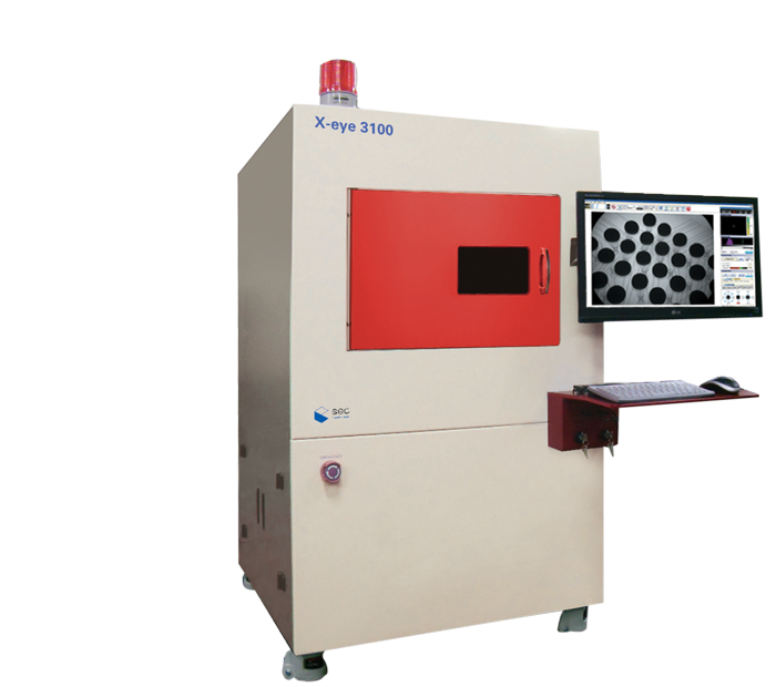
  • X-eye3100 tablesize350mm x 270mm
  • X-eye5100 tablesize460mm x 340mm
  • 100kV Micro-focus closed-tube (5um Focal Spot Size)
  • Flat Panel X-ray detector equipped
  • Max. 4-axis manipulator configuration (X, Y, Z, Tilt)
  • Auto teaching ( CNC Programming)
  • Various measuring tool & auto BGA inspection module

X-eye 6200 - X-ray Inspection System

Features

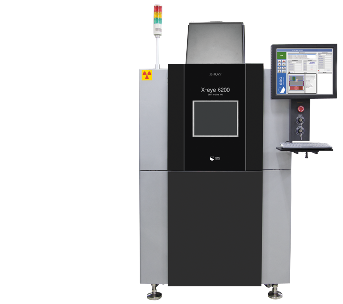
  • Automated In-line 2D X-ray Inspection
  • High detection of industrial demanding defect on PCB
  • Intuitive -Flexible Configuration
  • Easy to Program
  • Fast Throughput
  • Cost Effective

X-Eye SF 160 ACT - X-Ray 3D-CT System

Features

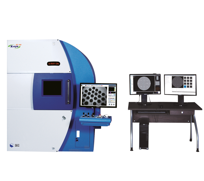
  • 160kV Micro-focus X-ray open tube with 1 micron focal spot size
  • 460mm x 510mm table size with full enhanced stroke axis (X,Y,Z,T,R)
  • Max. magnification up to 4,800x
  • Unparalleluser interface with various software tools
  • Micro-CT module & oblique CT scanning

SEC Korea

A dynamic, international and industrially active X-ray inspection company

DJK Europe and SEC Korea, are passionate about doing whatever it takes to help their customers succeed. Through the practical applications and knowledge of the two companies, they are developing innovative solutions to enable even smarter advances in the future.

In today's global industrial X-ray inspection environment, there is some demand for - but also trends towards - ultra-high resolution, 2D & 3D inline AXI, and low-cost technologies, including smaller than expected components such as nano- & micrometer miniaturization, package-on-package (PoP) and 3D packaging techniques. In addition, their flexible, affordable and practical options also offer significant added value, helping their customers to achieve their own progress.

The SEC product range

The X-eye160 and NF120 X-ray systems are among the flagship products in the SEC product range. These models are high-performance X-ray inspection systems that are used for general non-destructive testing and defect analysis.

The system is equipped with a 100 kV or 160 kV open/closed nano/microfocus X-ray tube and a high resolution flat panel detector. Thanks to the programmable multi-axis control system, the user can also view the object at any magnification - with excellent ease of use and with a so-called auto-teaching function with computerized numerical control (CNC programming), the system can practically be used as a semi-automatic inspection system. In this way, they can provide a user-friendly operating environment with numerous measuring and annotation tools.

The SF160 model in particular is a micro-focus X-ray system with high resolution that can be used to inspect electronic components (in the field of automotive assemblies), PCB assembly and semiconductors. Thanks to its superior X-ray imaging, even the smallest microscopic hidden defects can be detected in high resolution.
The SF160 model is equipped with an open microfocus tube with 160 kV and a spot size of 1 µm. The system allows the object to be magnified up to 4,800 times and the X-ray image can be displayed at any angle thanks to the six-axis manipulator configuration.

Using CT (computed tomography: 3D), all hidden structural and even microscopic defects within the object are visualized. Thanks to SEC's unique oblique CT technology, highly magnified CT images of even large samples can be produced. It is generally known that CT images are subject to certain limitations above a certain object size. Thanks to oblique CT technology, however, size limitations are no longer an issue, making PCB assemblies, large-format multilayer circuits and even semiconductor wafers suitable for this technology. Digital volume tomography (DVT) is generally used for CT analysis of electronic components. However, when analyzing flat and large components, such as printed circuit boards, CBCT has certain limitations in terms of generating highly magnified 3D images, which can be attributed to the large distance between the source and the object.

One of the core technologies is the nano-focus X-ray inspection system (0.4 micrometers), which enables SEC's customers to use ultra-high resolution images to inspect specific applications such as electronic component failure analysis, solder ball size status, voids and bridges, and more. This is especially true when inspecting the packaging of semiconductors (WLP: Wafer Level Packaging), balls and voids, checking the alignment of silicon vias (2D or 3D) and much more.

Customers are the beginning and the end of everything SEC does. They are aware of what their customers need, exceed their expectations in areas they care about, and pave the way for their success.

Kontakt

DJK Europe GmbH
Mergenthalerallee 79-81
65760 Eschborn, Germany
Phone: +49 6196 77614-15